- 您现在的位置:买卖IC网 > Sheet目录39249 > LM4867LQ/NOPB (NATIONAL SEMICONDUCTOR CORP) 3 W, 2 CHANNEL, AUDIO AMPLIFIER, PQCC24
Application Information (Continued)
T
JMAX =PDMAX
θ
JA +TA
(6)
Equation (6) gives the maximum junction temperature
T
JMAX. If the result violates the LM4867’s 150C, reduce the
maximum junction temperature by reducing the power sup-
ply voltage or increasing the load resistance. Further allow-
ance should be made for increased ambient temperatures.
The above examples assume that a device is a surface
mount part operating around the maximum power dissipation
point. Since internal power dissipation is a function of output
power, higher ambient temperatures are allowed as output
power or duty cycle decreases.
If the result of Equation (2) is greater than that of Equation
(3), then decrease the supply voltage, increase the load
impedance, or reduce the ambient temperature. If these
measures are insufficient, a heat sink can be added to
reduce
θ
JA. The heat sink can be created using additional
copper area around the package, with connections to the
ground pin(s), supply pin and amplifier output pins. External,
solder attached SMT heatsinks such as the Thermalloy
7106D can also improve power dissipation. When adding a
heat sink, the
θ
JA is the sum of
θ
JC,
θ
CS, and
θ
SA.(
θ
JC is the
junctiontocase
thermal
impedance,
θ
CS
is
the
casetosink
thermal
impedance,
and
θ
SA
is
the
sinktoambient thermal impedance.) Refer to the Typical
Performance Characteristics curves for power dissipation
information at lower output power levels.
POWER SUPPLY BYPASSING
As with any power amplifier, proper supply bypassing is
critical for low noise performance and high power supply
rejection. Applications that employ a 5V regulator typically
use a 10F in parallel with a 0.1F filter capacitors to stabi-
lize the regulator’s output, reduce noise on the supply line,
and improve the supply’s transient response. However, their
presence does not eliminate the need for a local 1.0F
tantalum bypass capacitance connected between the
LM4867’s supply pins and ground. Do not substitute a ce-
ramic capacitor for the tantalum. Doing so may cause oscil-
lation. Keep the length of leads and traces that connect
capacitors between the LM4867’s power supply pin and
ground as short as possible. Connecting a 1F capacitor,
C
B, between the BYPASS pin and ground improves the
internal bias voltage’s stability and improves the amplifier’s
PSRR. The PSRR improvements increase as the bypass pin
capacitor value increases. Too large, however, increases
turnon time and can compromise the amplifier’s click and
pop performance. The selection of bypass capacitor values,
especially C
B, depends on desired PSRR requirements,
click and pop performance (as explained in the section,
Proper Selection of External Components), system cost,
and size constraints.
MICROPOWER SHUTDOWN
The voltage applied to the SHUTDOWN pin controls the
LM4867’s shutdown function. Activate micropower shut-
down by applying V
DD to the SHUTDOWN pin. When active,
the LM4867’s micropower shutdown feature turns off the
amplifier’s bias circuitry, reducing the supply current. The
logic threshold is typically V
DD/2. The low 0.7A typical
shutdown current is achieved by applying a voltage that is as
near as V
DD as possible to the SHUTDOWN pin. A voltage
that is less than V
DD may increase the shutdown current.
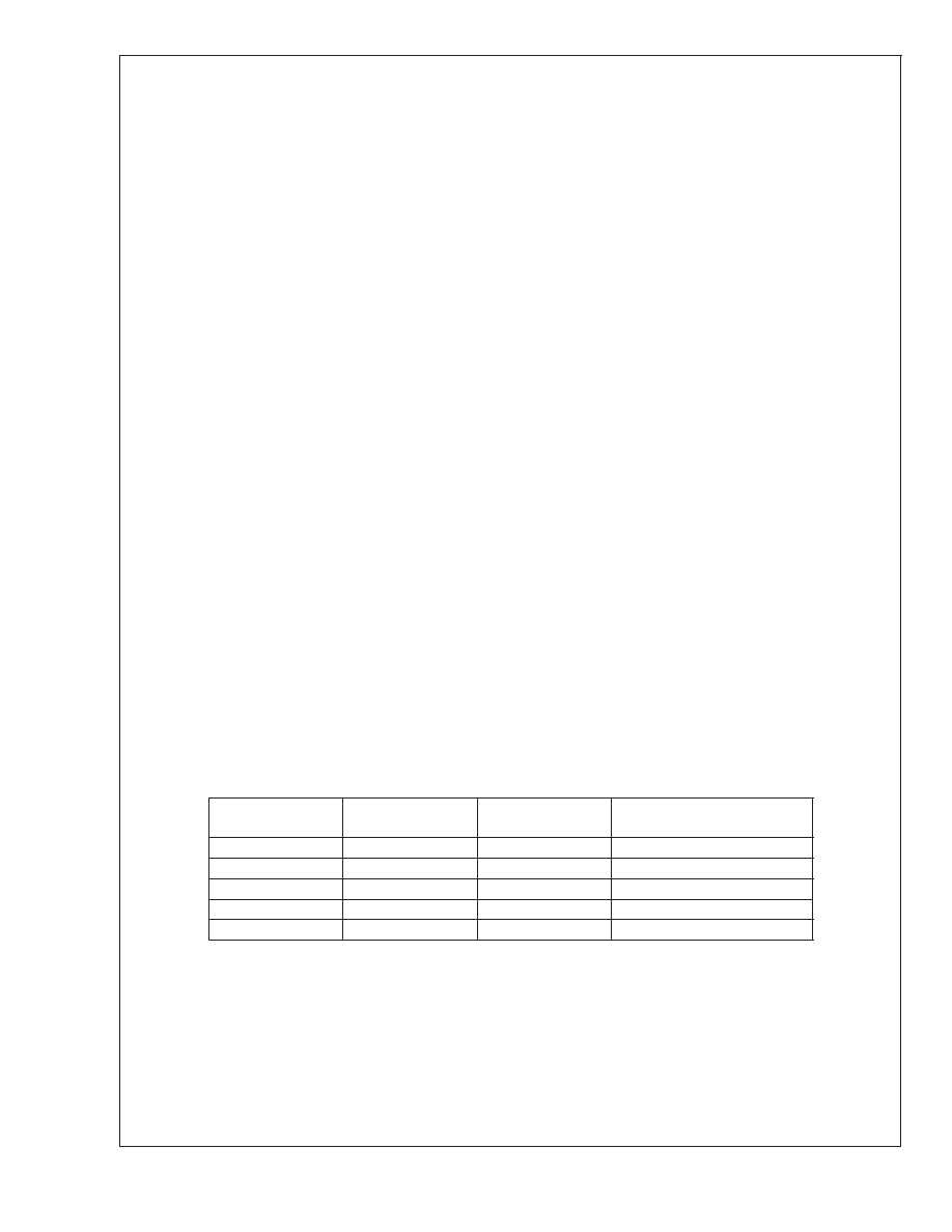
Table 1 shows the logic signal levels that activate and deac-
tivate micropower shutdown and headphone amplifier op-
eration. To ensure that the output signal remains
transientfree, do not cycle the shutdown function
faster than 1Hz.
There are a few ways to control the micropower shutdown.
These include using a singlepole, single, throw switch, a
microprocessor, or a microcontroller. When using a switch,
connect an external 100k
pullup resistor between the
SHUTDOWN pin and V
DD. Connect the switch between the
SHUTDOWN pin and ground. Select normal amplifier opera-
tion by closing the switch. Opening the switch connects the
SHUTDOWN pin to V
DD through the pullup resistor, acti-
vating micropower shutdown. The switch and resistor guar-
antee that the SHUTDOWN pin will not float. This prevents
unwanted state changes. In a system with a microprocessor
or a microcontroller, use a digital output to apply the control
voltage to the SHUTDOWN pin. Driving the SHUTDOWN pin
with active circuitry eliminates the pull up resistor.
Truth Table for Logic Inputs
SHUTDOWN
PIN
HP-IN
PIN
MUX CHANNEL
INPUT SELECT
OPERATIONAL MODE (MUX
INPUTCHANNEL #)
Logic Low
= OUTB signal
Logic Low
Bridged amplifiers (1)
Logic Low
= OUTB signal
Logic High
Bridged amplifiers (2)
Logic Low
≠ OUTB signal
Logic Low
Single-ended amplifiers (1)
Logic Low
≠ OUTB signal
Logic High
Single-ended amplifiers (2)
Logic High
X
Micropower shutdown
HEADPHONE (SINGLE-ENDED) AMPLIFIER
OPERATION
An internal pullup circuit is connected to the HPIN (pin 20)
headphone amplifier control pin. When this pin is left uncon-
nected, V
DD is applied to the HPIN. This turns off Amp2B
and switches Amp2A’s input signal from an audio signal to
the V
DD/2 voltage present on pin 14. The result is muted
bridge-connected loads. Quiescent current consumption is
reduced when the IC is in this singleended mode.
Figure 8 shows the implementation of the LM4867’s head-
phone control function. An internal comparator with a nomi-
nal 400mV offset monitors the signal present at the OUTB
output. It compares this signal against the signal applied to
the HPIN pin. When these signals are equal, as is the case
when a BTL is connected to the amplifier, the comparator
forces the LM4867 to maintain bridgedamplifier operation.
When the HPIN pin is externally floated, such as when
LM4867
www.national.com
16
发布紧急采购,3分钟左右您将得到回复。
相关PDF资料
LM4867LQX/NOPB
3 W, 2 CHANNEL, AUDIO AMPLIFIER, PQCC24
LM4882MM/NOPB
0.48 W, 1 CHANNEL, AUDIO AMPLIFIER, PDSO8
LM4882M/NOPB
0.48 W, 1 CHANNEL, AUDIO AMPLIFIER, PDSO8
LM556ICN
DUAL PULSE; RECTANGULAR, TIMER, PDIP14
LM5756
3.5 A SWITCHING REGULATOR, 100 kHz SWITCHING FREQ-MAX, ZFM5
LM7001JM
PLL FREQUENCY SYNTHESIZER, 130 MHz, PDSO20
LM7001M
PLL FREQUENCY SYNTHESIZER, 130 MHz, PDSO20
LM7006
PLL FREQUENCY SYNTHESIZER, 400 MHz, PDIP20
相关代理商/技术参数
LM4867MT
制造商:NSC 制造商全称:National Semiconductor 功能描述:Output-Transient-Free Dual 2.1W Audio Amplifier Plus No Coupling Capacitor Stereo Headphone Function
LM4867MT NOPB
制造商:Texas Instruments 功能描述:Audio Amp Headphone/Speaker 2-CH Stereo 1.5W Class-AB 20-Pin TSSOP Rail
LM4867MT/NOPB
功能描述:IC AMP AUDIO PWR 3W AB 20TSSOP RoHS:是 类别:集成电路 (IC) >> 线性 - 音頻放大器 系列:Boomer® 产品培训模块:Lead (SnPb) Finish for COTS
Obsolescence Mitigation Program 标准包装:2,500 系列:DirectDrive® 类型:H 类 输出类型:耳机,2-通道(立体声) 在某负载时最大输出功率 x 通道数量:35mW x 2 @ 16 欧姆 电源电压:1.62 V ~ 1.98 V 特点:I²C,麦克风,静音,短路保护,音量控制 安装类型:表面贴装 供应商设备封装:25-WLP(2.09x2.09) 封装/外壳:25-WFBGA,WLCSP 包装:带卷 (TR)
LM4867MTE
制造商:Texas Instruments 功能描述:Audio Amp Headphone/Speaker 2-CH Stereo 3W Class-AB 20-Pin TSSOP EP Rail
LM4867MTE/NOPB
功能描述:IC AMP AUDIO PWR 3W AB 20TSSOP RoHS:是 类别:集成电路 (IC) >> 线性 - 音頻放大器 系列:Boomer® 产品培训模块:Lead (SnPb) Finish for COTS
Obsolescence Mitigation Program 标准包装:2,500 系列:DirectDrive® 类型:H 类 输出类型:耳机,2-通道(立体声) 在某负载时最大输出功率 x 通道数量:35mW x 2 @ 16 欧姆 电源电压:1.62 V ~ 1.98 V 特点:I²C,麦克风,静音,短路保护,音量控制 安装类型:表面贴装 供应商设备封装:25-WLP(2.09x2.09) 封装/外壳:25-WFBGA,WLCSP 包装:带卷 (TR)
LM4867MTEX
制造商:National Semiconductor Corporation 功能描述:Audio Amplifier Circuit, Dual, 20 Pin, Plastic, TSSOP
LM4867MTEX/NOPB
功能描述:IC AMP AUDIO PWR 3W AB 20TSSOP RoHS:是 类别:集成电路 (IC) >> 线性 - 音頻放大器 系列:Boomer® 产品培训模块:Lead (SnPb) Finish for COTS
Obsolescence Mitigation Program 标准包装:2,500 系列:DirectDrive® 类型:H 类 输出类型:耳机,2-通道(立体声) 在某负载时最大输出功率 x 通道数量:35mW x 2 @ 16 欧姆 电源电压:1.62 V ~ 1.98 V 特点:I²C,麦克风,静音,短路保护,音量控制 安装类型:表面贴装 供应商设备封装:25-WLP(2.09x2.09) 封装/外壳:25-WFBGA,WLCSP 包装:带卷 (TR)
LM4867MTX/NOPB
功能描述:IC AMP AUDIO PWR 3W AB 20TSSOP RoHS:是 类别:集成电路 (IC) >> 线性 - 音頻放大器 系列:Boomer® 产品培训模块:Lead (SnPb) Finish for COTS
Obsolescence Mitigation Program 标准包装:2,500 系列:DirectDrive® 类型:H 类 输出类型:耳机,2-通道(立体声) 在某负载时最大输出功率 x 通道数量:35mW x 2 @ 16 欧姆 电源电压:1.62 V ~ 1.98 V 特点:I²C,麦克风,静音,短路保护,音量控制 安装类型:表面贴装 供应商设备封装:25-WLP(2.09x2.09) 封装/外壳:25-WFBGA,WLCSP 包装:带卷 (TR)